Simplify Portable Low-Power Audio Circuit Design Class D Amplifiers
This article will explain the difference between the various types of audio amplifiers, detail the theory of operation of Class D amplifiers, and show how they increase efficiency and reduce power requirements and size.
Audio circuits for handsets and portable IoT devices demand the vital characteristics of low power, small size, and low heat dissipation. However, audio amplifiers are often inefficient heat generators that require bulky heatsinks. To reduce size and power requirements, Class D, or digital amplifiers, offer a good solution.
What the switched mode power supply brought to power sources, the Class D amplifier brings to audio playback. With Class D amplifiers, audio inputs are encoded as pulse width modulated (PWM) signals that drive the power devices between on and off levels, with power only being dissipated during the transitions.
These “digital” amplifiers greatly increase the efficiency of audio amps, resulting in lower heat dissipation and smaller physical size. Also, recent developments have changed the modulation schemes so that low-pass filters are no longer required at the outputs, further reducing size and complexity.
Analog power amplifiers
The development of analog power amplifiers has been focused on improving fidelity while at the same time improving amplifier efficiency. Amplifiers are classified by the letters A, B, AB, or C based upon their operating or bias point, and the percentage of the input signal cycle over which they conduct (Figure 1).

Figure 1: The operating bias and signal conduction of Class A, B, AB, and C analog amplifiers. (Image source: Digi-Key Electronics)
Class A amplifiers (upper left) conduct during the whole cycle of the input signal. They are biased at the midpoint of the input-output operating characteristics. The signal fidelity is excellent, but because the amplifier is always on, even with no input signal, the efficiency tends to be low.
Class B (lower left) amplifiers are intended to improve efficiency by biasing the amplifier at cutoff. The amplifier only conducts for half the input cycle. Normally the circuit is configured in a push-pull topology to amplify both positive and negative input transitions. With no signal present the amplifier is not conducting, raising its efficiency. This advantage is countered by a loss in fidelity due to crossover distortion which can occur at the transition points of input polarity.
The crossover distortion issue can be addressed by moving the bias point of the amplifier slightly higher. This results in the Class AB amplifier (upper right). This type of amplifier is also generally used in a push-pull configuration. The Class AB amplifier is the most common type for audio power applications.
The Class C amplifier (lower right) is designed to conduct over a very small portion of the input cycle. It is characterized by high efficiency, but its fidelity is poor. These amplifiers find application in RF power designs where the output load is a resonant circuit which recovers the correct waveform.
Strategies to improve the efficiency of these analog amplifiers are focused on reducing the conduction phase of the amplifier to the smallest possible duration, as shown with the Class C amplifier.
Class D basics
The Class D amplifier takes a different approach and instead operates much like a switched mode power supply (Figure 2).

Figure 2: A Class D amplifier converts the analog input into a PWM waveform to drive FET switches full on or off. The output low-pass filter recovers the analog waveform at the speaker. (Image source: Digi-Key Electronics)
The Class D amplifier converts the input analog signal into a pulse width modulated (PWM) waveform. The PWM waveform drives the push-pull FET output stage fully on or off for each pulse. When one of the FETs is on, the current through it is high, but the voltage across it is very low, so power is only dissipated during the brief transitions between the on and off state. Likewise, when the FET is off, the voltage across it is high, but the current is near zero. Again, there is no power dissipation except in the state transitions.
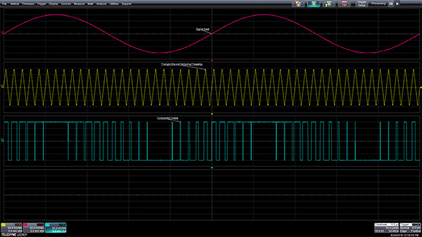
Conversion of the analog waveform into a PWM waveform is done by applying the analog waveform to one input of a comparator while a triangle or ramp waveform, at the desired switching frequency, is applied to the other input (Figure 3). The upper trace represents the input waveform, in this case a 10 kilohertz (kHz) sinewave, which is applied to one input of a comparator. The center trace is a 250 kHz triangle wave which is applied to the other comparator input. The output of the comparator is the PWM waveform shown in the lower trace. The pulse width varies with the amplitude of the input signal.

Figure 3: Creating a PWM signal from the analog input requires the input signal (top) and a triangle or ramp function (middle). Both are then applied to the inputs of a comparator to produce a PWM signal with pulse widths that vary according to the input signal amplitude (bottom). (Image source: Digi-Key Electronics)
The output of the FET push-pull power stage is also a PWM signal. This is applied to a simple inductor-capacitor (L-C) low-pass filter to recover the amplified analog waveform. The frequency of the triangle wave has to be much higher than the corner frequency of the low-pass filter.
An alternative to PWM is pulse density modulation (PDM). PDM uses a series of short duration rectangular pulses, the density of which varies as a function of the analog input amplitude. It is generated using sigma-delta modulation.
The gain of the Class D amplifier is affected by the bus voltages. While it has a poor power supply rejection ratio, it is corrected by using feedback around the amplifier. This is shown in the block diagram of Figure 2, where feedback is taken from the filter input.
The key benefit of the Class D amplifier is its high efficiency of about 90%. This is much better than its closest analog rival, the Class AB amplifier, with an efficiency of 50 to 70%.
High efficiency enables smaller physical size and possibly the elimination of heatsinks and cooling fans. When applied in portable devices, higher efficiency translates into longer battery life. Efficiency varies directly with output power levels and falls with decreasing power.
Class D amplifier topologies
There are two topologies generally used for the Class D amplifiers, the simpler of the two is the half-bridge circuit shown in Figure 4.

Figure 4: The two commonly used Class D topologies are the half-bridge and the full-bridge configuration. (Image source: Digi-Key Electronics)
The full-bridge topology, referred to as the bridge-tied load (BTL), offers the benefit of higher output power for the same supply voltages as the half-bridge configuration. The half-bridge has the filter input swinging between either the positive or negative power rails, while the BTL circuit has the load between the positive and negative rails simultaneously doubling the applied voltage to the load, thus quadrupling the power output. BTL operation also allows the use of a single unipolar power supply.
Filterless Class D amplifiers
With the traditional Class D switching system, called AD modulation, the duty cycle modulates the rectangular waveform such that its average value corresponds to the input analog signal voltage. The BTL outputs complement each other. There is no significant common-mode switching content in its output. However, there is a common-mode DC voltage due to the average value of the PWM switching. Since this DC voltage level is applied to both sides of the load, it does not add to power dissipation across it.
With no input, the amplifier switches at its nominal PWM frequency with a 50% duty cycle applied to the load. This causes significant current flow and power dissipation in the load. The L-C filter is necessary to lower the current to a “ripple” for improved efficiency. The lower this ripple current, the better the efficiency due to reduced dissipation at the load and reduced conduction losses across RDS(on) of the output FETs.
An alternative modulation scheme, often referred to as BD or filterless modulation, uses a switching system that modulates the duty cycle of the difference of the output signals so that its average value matches the input analog signal. The BTL outputs are in phase with each other when idle, not complimentary. This results in zero voltage difference across the load, minimizing the quiescent power consumption without the need of a filter. BD modulation has significant common-mode content in its output. This modulation scheme relies on the intrinsic inductance of the loudspeaker and the bandpass filter characteristic of the human ear to recover the audio signal.
Class D amplifier integrated circuits
The Texas Instruments TPA3116D2DADR is a Class D stereo amplifier which has > 90% efficiency and supports multiple output power configurations, including 2 channels at 50 watts into a 4 Ω BTL load at 21 volts. Other models in the family support 2 channels at 30 watts into 8 Ω at 24 volts, and 2 channels at 15 watts into 8 Ω at 15 volts. Only the highest power device requires a heatsink.
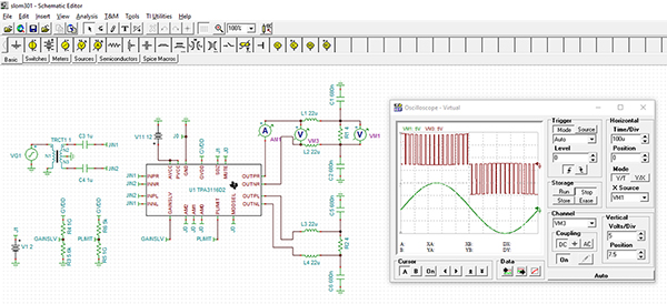
The devices support switching frequencies up to 1.2 MHz with AM avoidance to prevent interference. A choice of AD or BD modulation schemes is selectable via a single input control. It includes integrated self-protection circuits including over voltage, under voltage, over temperature, DC detect, and short circuit with error reporting. A typical configuration is shown using TI’s TINA-TI simulation tool (Figure 5).
Figure 5: A TI TPA3116D2DADR Class D stereo amplifier simulation showing the raw (VM3) and filtered (VM1) output waveforms for BD modulation. (Image source: Digi-Key Electronics)
The circuit uses a single 12 volt supply and shows an output power level of 12.5 watts into 4 Ω. The virtual oscilloscope shows the raw digital output (VM3) as well as the filtered output (VM1).
The Texas Instruments TPA3126D2DAD is a performance upgrade to the TPA3116D2 series. The device is pin-to-pin compatible with the older IC and features a major improvement that reduces the idle current by 70% using a proprietary hybrid modulation scheme. The scheme reduces idle current at low power levels to extend battery life.
Low-power operation requires more care in the design of Class D amplifiers. As mentioned previously, efficiency is proportional to power level, and low power levels generally mean lower efficiency. The Texas Instruments TPA2001D2PWPR is a 1 watt per channel stereo Class D amplifier that is a third-generation Class D design. It features lower supply current, lower noise floor, and better efficiency. Designed around the Class D filterless modulation scheme, it does not require an output filter, saving the designer parts cost and board space. It can deliver more than 1 watt per channel into 8 Ω using a 5 volt supply.
A reference design is available as an evaluation board, the TPA2001D2EVM, forming a plug-and-play Class D audio amplifier (Figure 6).

Figure 6: A 1 watt per channel stereo amplifier based on the TPA2001D2 Class D amplifier. (Image source: Texas Instruments)
The amplifier, using BTL topology, is basically self-contained requiring only a few external components.
Conclusion
Class D amplifiers offer low losses and very high-power efficiency in a small package for portable and battery-powered designs. Off-the-shelf ICs make applying these amplifiers fast and easy, and recent advances have reduced the need for filters, making them less expensive and more compact.


Comment